FLUORESCENCE MICROSCOPE
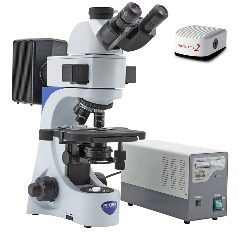
A fluorescence microscope is an optical microscope that uses fluorescence and phosphorescence instead of, or in addition to, reflection and absorption to study properties of organic or inorganic substances.
Principle:
The specimen is illuminated with light of a specific wavelength (or wavelengths) which is absorbed by the fluorophores, causing them to emit light of longer wavelengths (i.e., of a different color than the absorbed light). The illumination light is separated from the much weaker emitted fluorescence through the use of a spectral emission filter. Typical components of a fluorescence microscope are a light source (xenon arc lamp or mercury-vapor lamp), the excitation filter, the dichroic mirror (or dichroic beamsplitter), and the emission filter (see figure below). The filters and the dichroic are chosen to match the spectral excitation and emission characteristics of the fluorophore used to label the specimen. In this manner, the distribution of a single fluorophore (color) is imaged at a time. Multi-color images of several types of fluorophores must be composed by combining several single-color images

Scanning Electron Microscope
A scanning electron microscope (SEM) scans a focused electron beam over a surface to create an image. The electrons in the beam interact with the sample, producing various signals that can be used to obtain information about the surface topography and composition.
The electron beam is scanned in a raster scan pattern, and the position of the beam is combined with the intensity of the detected signal to produce an image. In the most common SEM mode, secondary electrons emitted by atoms excited by the electron beam are detected using an Everhart-Thornley detector. The number of secondary electrons that can be detected, and thus the signal intensity, depends, among other things, on specimen topography.

Transmission Electron Microscope
Transmission Electron Microscope is a microscopy technique in which a beam of electrons is transmitted through a specimen to form an image. The specimen is most often an ultrathin section less than 100 nm thick or a suspension on a grid. An image is formed from the interaction of the electrons with the sample as the beam is transmitted through the specimen. The image is then magnified and focused onto an imaging device, such as a fluorescent screen, a layer of photographic film, or a sensor such as a scintillator attached to a charge-coupled device.
Electron microscopes enable clear observation of micro-structures, which is not possible with optical microscopes. Moreover, they also make it possible to analyze substance structures and obtain atomic level information by using an electron beam. The electron microscope is an epoch-making invention used throughout the world to investigate an atomic world that we could hardly imagine.

Confocal Microscope
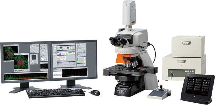
Confocal Microscope is an optical imaging technique for increasing optical resolution and contrast of a micrograph by means of using a spatial pinhole to block out-of-focus light in image formation.
Capturing multiple two-dimensional images at different depths in a sample enables the reconstruction of three-dimensional structures (a process known as optical sectioning) within an object.
Confocal microscope that captures images with a 25 mm field of view, nearly twice the area of conventional point scanners

Atomic Force Microscope
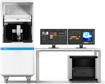
Atomic Force Microscope is a very-high-resolution type of scanning probe microscopy (SPM), with demonstrated resolution on the order of fractions of a nanometer, more than 1000 times better than the optical diffraction limit.
AFM provides accurate measurement at highest nanoscale resolution than any other products in its class.It allows you to obtain sample images and its characteristic measurements true to its nano structure thanks to its flat, orthogonal, and linear scan measurements by its unique AFM architecture: independent XY and Z, flexure based scans.

Atomic Force Microscope SICM Module
The AFM has been applied to problems in a wide range of disciplines of the natural sciences, including solid-state physics, semiconductor science and technology, molecular engineering, polymer chemistry and physics, surface chemistry, molecular biology, cell biology, and medicine.
The integration of the SICM and AFM system allows researchers to expand the depth of their research and easily perform nanoscale imaging in aqueous environments.
- SICM Standard Imaging
- DC (direct current) mode, ARS (apporach-retract-scan) mode
- SICM Ionic Current Measurement
